Product-Proven Binary Masks
Solutions Where You Need Them
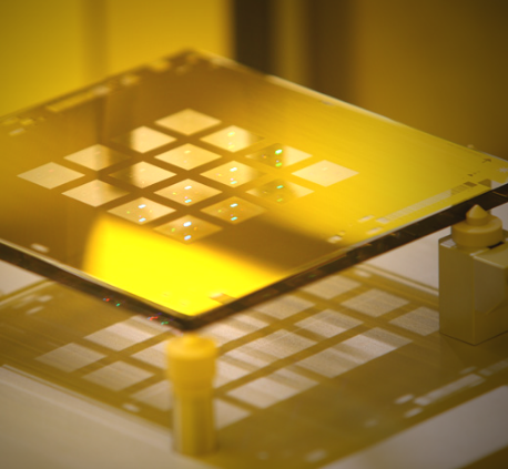
Our worldwide manufacturing facilities provide local solutions for reduction reticles (primarily 2X to 5X), Ultratech 1X reticles, and Standard 1X photomasks—along with a range of mask sizes from 4 to 14 inches for integrated circuit manufacturing. We also supply 1X masters and copies, with optional anti-stick coatings. Equipment sets are optimized for fast cycle time and low cost, without compromising quality.
Extend Your Legacy Tools
With solid roots in legacy technologies, our mature binary mask solutions are in volume production to support your wafer printing needs for a variety of applications. This allows you to maximize ROI by extending the use of your incumbent lithography systems.

Advanced Binary OPC Masks
Pushing Technology Nodes
At Photronics, we’ve stayed in step with lithography advancements as the semiconductor industry continues to push the lithography limits with extreme low-k1 processing and the effects of high mask error enhancement factor (MEEF) lithography.
Our advanced binary reticles easily support production nodes from 14nm to 28nm, with development and innovation at 7nm and below, including EUV, clearly in our sights.
Key Considerations
- E-beam lithography tools and chemically amplified resist (CAR) resolve very small main and OPC features on the mask.
- Advanced laser lithography tools provide a lower-cost solution when ultimate resolution is less critical.
- Dry-etch ensures pattern fidelity by minimizing CD loss as the resist pattern is transferred to the chrome absorber layer.
Common Specifications
| Binary Photomasks | ||||
|---|---|---|---|---|
| Standard binary photomasks are typically used for 1X, 2X 2.5X, 4X and 5X applications |
||||
| Mask sizes range from 4"x4" to 9"x9" | ||||
| Common Specifications for Binary masks, of course we will work with our customers if tighter requirements are needed |
||||
| CD Size | CD Tolerance | CD Uniformity | Registration | Defect Size |
| 1.0-2.0μ | ±1.5μ | .15μ | ±.15μ | .50μ |
| >2.0μ | ±.20μ | .20μ | ±.15μ | 1.0μ |
| Advanced Binary Photomasks | ||||
|---|---|---|---|---|
| Advanced Binary photomasks are typically used for 1X, 4X and 5X applications | ||||
| Mask size is typically 6"x6" | ||||
| Common Specifications for Advanced Binary masks, of course we will work with our customers if tighter requirements are needed | ||||
| CD Size | CD Tolerance | CD Uniformity | Registration | Defect Size |
| .50μ-1.0μ | ±.035μ | .035μ | ±.03μ | .20μ |
| >1.0μ | ±.05μ | .05μ | ±.05μ | .03μ |
| Large Area Photomasks | ||||
|---|---|---|---|---|
| Mask size raging from 9"x9" up to 24"x30" | ||||
| Common Specifications for LAM, of course we will work with our customers if tighter requirements are needed |
||||
| CD Size | CD Tolerance | CD Uniformity | Registration | Defect Size |
| >2.0μ | ±.50μ | .50μ | ±1.0μ | 1.0μ |
Specialty Phase-Shift Masks
Better Resolution and DOF
At 248nm and 193nm wavelengths, our embedded attenuated phase-shift masks (EAPSM) rely on a wavelength-tuned, 6% transmission MoSiON absorber to produce a 180-degree phase shift. This improves a lithography tool’s resolution and depth of focus.
EUV Masks
After years of waiting, extreme ultraviolet (EUV) capability is finally in production, and with it the ability to take technology nodes to 5nm feature sizes and beyond. Our R&D team has played an important role in this next-generation lithography development, including a joint R&D agreement with IBM Research to develop manufacturing-grade EUV mask processes for leading-edge logic applications for 7nm and 5nm nodes, and beyond. As a result, our technology portfolio is poised to meet aggressive ramp schedules when EUV photomasks become mainstream.
Key Considerations
- Define the top chrome layer using leading-edge e-beam or laser patterning tools.
- Create a pattern for the MoSiON below the top chrome layer using an inductively coupled plasma (ICP) dry-etch process.
- Define the active phase-shift pattern area by recoating the mask with resist and performing a second-level exposure with the laser patterning tool. The mask fiducials, barcode and titles are left in high-contrast chrome.
- Repair critical defects (CDs) using precision-beam or atomic-force microscope tools.
- Verify CDs using aerial image metrology (AIMS).
- Minimize the risk of exposure-dependent haze defects with proprietary cleaning and treatment.
Committed to Green
At Photronics, we are committed to protecting our environment. That’s why, together with our customers and blank suppliers, we created a quartz substrate reclamation program. With customer approval, we recycle and reuse substrates for less critical applications. Through this program, we have successfully reduced waste while also protecting the intellectual property of our customers.
In addition to the substrate reclamation program, we also reuse compacts.